
How Cerebras AI Chips Differ from NVIDIA GPUs
Cerebras is an artificial intelligence infrastructure company that bypasses traditional data-transfer bottlenecks by printing 900,000 compute cores and 44 gigabytes of memory onto a single, unbroken silicon wafer. By eliminating the need to shuttle data between smaller, separate chips, Cerebras achieves inference speeds up to 21 times faster than NVIDIA's standard graphics processing units (GPUs). However, to truly challenge NVIDIA's dominance, Cerebras must convince the industry to adopt its radically demanding liquid-cooled server racks and diversify a revenue base that relies heavily on a handful of sovereign and corporate partners.
The Bottleneck in Modern AI: The Memory Wall
To understand why a company would attempt to build a computer chip the size of a dinner plate, it is necessary to understand the primary physical constraint governing artificial intelligence today. That constraint is not a lack of mathematical processing power; it is the "memory wall."
For the last several decades, the semiconductor industry has successfully shrunk the size of transistors, allowing for explosive growth in raw computational capabilities. However, the speed at which data can be transferred between a computer's processor and its external memory has not kept pace. In modern generative AI, this disparity creates a massive bottleneck. When a large language model (LLM) generates a response, it undergoes a process called inference. During the "decode" stage of inference - where the model predicts the sequence's very next word or token - the hardware must read the model's entire set of weights from memory and feed them into the compute cores 1.
If an enterprise is running a 70-billion parameter model using 16-bit precision, the model's weights alone consume about 140 gigabytes of data 1. To generate a single word, that entire 140-gigabyte package must be swept through the processor. Traditional GPUs, such as NVIDIA's highly successful H100 or the newer Blackwell B200, contain an abundance of compute capacity. Yet, during single-user inference tasks, their math-crunching cores often sit idle, waiting for data to travel over the microscopic wires connecting the GPU to its external High-Bandwidth Memory (HBM) 12.
As the artificial intelligence industry matures, inference has overtaken training as the dominant workload, accounting for roughly two-thirds of all AI compute by early 2026 3. Models are trained once over the course of weeks or months, but they are subsequently deployed to serve millions of requests continuously 3. Complex "agentic" applications, where an AI might chain dozens of logical reasoning steps together before presenting a final answer to the user, require near-instantaneous token generation 45. When the model stalls mid-thought because the hardware is struggling to shuttle data from memory to processor, the user experience breaks down 4. Cerebras was founded on the premise that the only way to tear down the memory wall is to fundamentally reimagine the physical structure of the semiconductor.
The Cerebras Wafer-Scale Engine (WSE-3)
Standard semiconductor manufacturing is a highly standardized, sequential process. Foundries like the Taiwan Semiconductor Manufacturing Company (TSMC) fabricate complex circuitry onto 300-millimeter circular silicon wafers. Once the etching is complete, the wafer undergoes testing to locate microscopic defects, which are inevitable in advanced manufacturing. Finally, the wafer is sliced - or "diced" - into hundreds of individual rectangular chips 6. The defective chips are discarded, and the functional ones are placed into protective packaging to be wired into computers 6. The maximum size of these individual chips is physically constrained to roughly 800 square millimeters by the "reticle limit" of the lithography equipment used to print them 67.
Cerebras subverts this paradigm entirely by skipping the dicing phase. It utilizes the largest square that can be mapped onto a 300-millimeter silicon wafer as a single, monolithic processor 81.
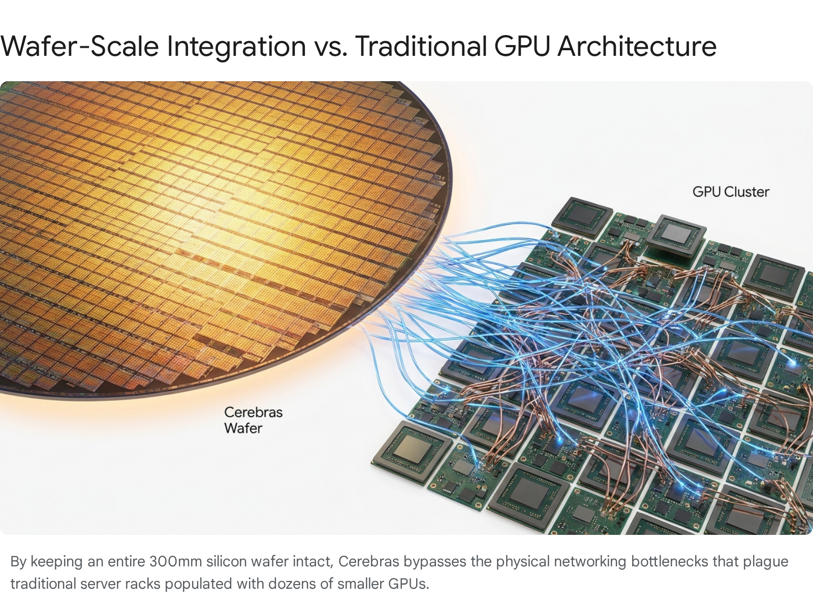
The company's third-generation hardware, the Wafer-Scale Engine 3 (WSE-3), was released in 2024 and powers the CS-3 system. Fabricated on TSMC's 5-nanometer process node, the WSE-3 measures 46,225 square millimeters - approximately 57 times the physical size of an NVIDIA H100 GPU 110. This vast expanse of silicon houses 4 trillion transistors 1112.
The Defect-Tolerant Architecture
The primary reason the semiconductor industry traditionally avoided wafer-scale chips is the inevitability of manufacturing defects. A single speck of dust or crystal imperfection can ruin a circuit. On a standard reticle-sized chip, a defect means tossing a few square millimeters of silicon into the recycling bin. On a wafer-scale chip, a single defect would theoretically render the entire dinner-plate-sized processor useless, making production economically impossible 1.
Cerebras solved this by engineering a hardware architecture explicitly designed to expect and route around failure. The WSE-3 is manufactured with roughly 970,000 microscopic physical compute cores. During post-fabrication testing, the system maps out any defective zones 1. The system's internal networking fabric then permanently deactivates the flawed cores, routing data around them seamlessly to guarantee an operational yield of exactly 900,000 functional AI cores per wafer 113.
Massive On-Chip SRAM Bandwidth
By preserving the wafer as a single unit, Cerebras is able to place its memory directly adjacent to its compute logic. Every one of the WSE-3's 900,000 cores has its own dedicated 48 kilobytes of Static Random-Access Memory (SRAM), totaling 44 gigabytes of memory distributed evenly across the chip 111.
SRAM is significantly faster than the external Dynamic Random-Access Memory (DRAM) or High-Bandwidth Memory (HBM) utilized by traditional GPUs, but it is notoriously expensive and takes up substantial physical real estate 114. Because Cerebras's cores and memory are physically separated by mere micrometers rather than inches of copper wiring, the WSE-3 achieves a staggering aggregate internal memory bandwidth of 21 petabytes per second 111. For comparison, this memory bandwidth is roughly 2,600 times faster than the bandwidth available on NVIDIA's flagship Blackwell B200 GPU 12. It is this unfathomable internal speed that allows Cerebras to shatter the memory wall and claim industry-leading inference metrics.
NVIDIA's Approach: Advanced Packaging and Rack-Scale Computing
NVIDIA's strategy stands in stark contrast to Cerebras. Rather than challenging the fundamental rules of silicon manufacturing, NVIDIA has mastered the art of advanced packaging - taking smaller, highly optimized discrete chips and stitching them together with unparalleled networking technology.
NVIDIA's graphics processing units are strictly bound by TSMC's reticle limits. To deliver massive generational performance leaps, NVIDIA has shifted toward "chiplet" designs. The Blackwell B200 GPU, for instance, consists of two large compute dies fused together on a single package alongside 192 gigabytes of HBM3e memory, yielding 208 billion transistors and a memory bandwidth of 8 terabytes per second 1516.
However, the rapid pace of artificial intelligence development has accelerated NVIDIA's hardware cadence. At the CES technology convention in January 2026, CEO Jensen Huang announced that the successor to Blackwell - the Vera Rubin platform - had already entered full production, targeting volume shipments for the second half of the year 1617.
The Vera Rubin R200 Architecture
The Rubin R200 GPU represents a profound leap in density and memory capability. Fabricated on TSMC's cutting-edge 3-nanometer process, a single Rubin GPU houses 336 billion transistors - a 1.6x increase over the Blackwell generation 1517. More importantly for inference workloads, Rubin transitions the industry to next-generation HBM4 memory. Each Rubin GPU carries 288 gigabytes of HBM4 across eight stacks, pushing memory bandwidth to 22 terabytes per second 1517.
While a jump to 22 terabytes per second is a massive achievement for off-chip memory, it remains orders of magnitude lower than Cerebras's 21 petabytes per second of on-chip SRAM bandwidth 1215. NVIDIA compensates for this per-chip bandwidth limitation through sheer scale and interconnect superiority.
Because a single NVIDIA GPU cannot hold a trillion-parameter frontier model, NVIDIA builds the "cluster as the computer." Through its proprietary NVLink technology, NVIDIA connects dozens of GPUs together to share workloads. The Rubin generation introduces NVLink 6, offering 3.6 terabytes per second of bidirectional communication between GPUs 1516. NVIDIA's primary deployment unit is the NVL72 rack - a single, liquid-cooled cabinet containing 72 Rubin GPUs and 36 Vera CPUs, acting logically as one massive supercomputer capable of 3.6 ExaFLOPS of low-precision inference compute 1718.
Architectural Comparison: Hardware by the Numbers
To understand the diverging philosophies of these two hardware giants, it is helpful to view their flagship architectures side-by-side. Cerebras optimizes for the elimination of interconnects, while NVIDIA optimizes for modularity, low-precision math, and enormous pools of slower, but vastly more capacious, external memory.
| Specification / Feature | Cerebras WSE-3 (CS-3 System) | NVIDIA Blackwell B200 | NVIDIA Rubin R200 |
|---|---|---|---|
| Transistor Count | 4 Trillion | 208 Billion | 336 Billion |
| Manufacturing Node | TSMC 5nm | TSMC 4NP | TSMC 3nm |
| Die Area | 46,225 mm2 | ~1,600 mm2 (Dual-die) | Near-reticle (Dual-die) |
| Primary Memory Type | On-chip SRAM | Off-chip HBM3e | Off-chip HBM4 |
| Memory Capacity (Per Unit) | 44 GB | 192 GB | 288 GB |
| Memory Bandwidth | 21 Petabytes/sec | 8 Terabytes/sec | 22 Terabytes/sec |
| Interconnect Strategy | On-wafer 2D silicon mesh | NVLink 5 (1.8 TB/s) | NVLink 6 (3.6 TB/s) |
| Power Envelope (Per Unit) | ~23 kW - 27 kW | ~1.0 kW - 1.2 kW | ~1.8 kW - 2.3 kW |
Sources: 1711151617
The "Feldman Formula" and the Reality of FLOPs
When comparing raw mathematical capability - measured in Floating-Point Operations Per Second (FLOPS) - the marketing materials from both companies require careful decryption. Cerebras advertises the WSE-3 as delivering 125 PetaFLOPS of AI compute at 16-bit (FP16) precision 114.
However, semiconductor analysts frequently note that this 125 PetaFLOPS figure relies on "sparse" calculations. In sparse computing, the hardware utilizes algorithms to dynamically skip multiplying numbers by zero, theoretically saving vast amounts of time 1. Cerebras assumes a highly aggressive 8:1 unstructured sparsity ratio to achieve its headline performance numbers, a calculation metric independent analysts have dubbed "Feldman's Formula" after Cerebras CEO Andrew Feldman 14.
When evaluated on "dense" computing - where the processor executes every math operation sequentially without skipping zeros, which is how NVIDIA typically benchmarks its base performance - the WSE-3's actual throughput drops to roughly 15.6 PetaFLOPS of FP16 compute 14. By contrast, a single NVIDIA Rubin GPU delivers up to 50 PetaFLOPS of dense inference compute utilizing NVIDIA's newer, highly efficient 4-bit (FP4) precision 1417.
This underscores a fundamental truth about the Cerebras architecture: the WSE-3 does not win by possessing the highest number of raw, dense calculators per square millimeter. It wins because its 900,000 calculators are never starved for data 214.
The Inference Race: Tokens Per Second
In the real-world application of artificial intelligence, theoretical FLOPS matter less than "tokens per second" - the rate at which a system can ingest a prompt and stream out generated text 10. For latency-critical applications, such as real-time voice assistants, autonomous agents, and live code generation, high throughput is the ultimate product differentiator 45.
Because the WSE-3 keeps the entire AI model - or significant portions of it - resident within its 44 gigabytes of on-chip SRAM, it achieves unprecedented inference speeds 12. In independent benchmarks, the Cerebras CS-3 system generated text using Meta's Llama 4 Maverick model at a staggering 2,522 tokens per second per user 1.
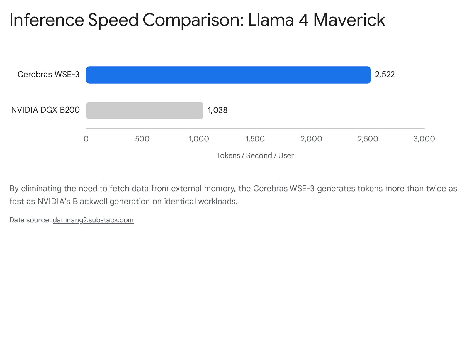
When tested on similar parameters, an NVIDIA DGX B200 system running the same model managed 1,038 tokens per second 1. Furthermore, on the massive 120-billion parameter open-weight model from OpenAI (gpt-oss-120B), Cerebras sustained roughly 2,700 tokens per second compared to just 900 tokens per second on a Blackwell B200 5.
NVIDIA counteracts this individual speed deficit through massive parallelization. A single NVIDIA GPU may take longer to serve one user, but a connected cluster of H200 or B200 GPUs can leverage their massive 141 GB or 192 GB external memory banks to process enormous "batches" of thousands of users concurrently 23. Cerebras, functioning as the ultimate low-latency engine, trades aggregate batch throughput for raw, single-user speed 2.
The "Stranded Silicon" Island Problem
Cerebras's reliance on SRAM introduces a critical physical limitation known within semiconductor engineering circles as the "stranded silicon" or "island" problem 2.
While the WSE-3 possesses an internal memory bandwidth of 21 petabytes per second, its external Input/Output (I/O) networking connection to the outside world is constrained to roughly 150 gigabytes per second via standard Ethernet connections 14. The wafer is essentially a Ferrari trapped on an island accessible only by a narrow dirt road 2.
If an AI model fits entirely within the 44 gigabytes of on-chip SRAM, the performance is flawless. However, if a model's parameters exceed 44 GB, Cerebras cannot rapidly stream the data on and off the chip without immediately encountering a severe latency choke point 214. Consequently, to maintain its speed advantage on modern, massive LLMs, Cerebras engineers must aggressively distill and compress multi-trillion-parameter models to ensure they fit natively on the die, or rely on highly complex pipeline parallelism to string multiple wafers together 2.
Training at Extreme Scale: MemoryX and SwarmX
If the WSE-3 is limited to 44 gigabytes of on-chip memory, how can it train trillion-parameter models that require terabytes of storage space?
For AI training workflows, Cerebras engineered a disaggregated hardware ecosystem that separates compute from memory storage. The company developed external hardware called MemoryX, a massive data vault comprising both DRAM and Flash storage capable of holding up to 2.4 petabytes of model weights 1920.
During training, the MemoryX unit streams the neural network weights into the WSE-3 one distinct layer at a time. The WSE-3 crunches the math using the data currently residing on the wafer, calculates the gradient updates, and sends the results back to the MemoryX unit via a custom networking fabric known as SwarmX 2122.
This "Weight Streaming" execution model drastically simplifies the software engineering required to train large models. Training a 175-billion parameter model on a cluster of thousands of NVIDIA GPUs typically demands tens of thousands of lines of distributed training code, forcing developers to slice the model into complex fractions using tensor, pipeline, and data parallelism 620. With Cerebras, because a single layer of even a multi-trillion parameter model can fit entirely on the 46,225-square-millimeter wafer, all parallelism defaults to pure "data parallelism" 71920.
Using Cerebras's built-in "Appliance Mode," developers can scale a training run from a single CS-3 system to a cluster of up to 2,048 systems by literally changing a single numerical parameter in their configuration code, achieving near-linear performance scaling without the gradient synchronization degradation that plagues traditional GPU clusters 6820.
Data Center Reality: Powering and Cooling the Monolith
The physical reality of housing a wafer-scale engine is a significant hurdle for enterprise adoption. You cannot simply slide a Cerebras CS-3 into a standard, air-cooled data center rack and plug it into a wall outlet.
An NVIDIA DGX B200 system operates within highly manageable electrical parameters, drawing approximately 14.3 kilowatts of power for an entire server node 113. In contrast, the Cerebras CS-3 system concentrates an immense 25 to 27 kilowatts of heat into a single piece of silicon operating in a 15U chassis 12.
Powering 4 trillion transistors simultaneously requires delivering roughly 30,000 amps of electrical current to the chip 2. Because standard peripheral power supplies would melt under this load, Cerebras engineered a custom 3D vertical power distribution system, placing dense arrays of voltage regulators on the front face of the board directly adjacent to the silicon 72.
Cooling this concentrated inferno requires specialized infrastructure. The CS-3 mandates a dedicated liquid cooling loop featuring redundant pumps pushing cold facility water at extreme flow rates of up to 4.0 liters per minute, frequently requiring 5-degree Celsius chilled water 21. As data center experts describe it, installing a Cerebras system is akin to "plumbing a commercial freezer directly onto a microchip" 2. This bespoke physical footprint means facilities must be aggressively retrofitted to accommodate the hardware, adding capital expenditure friction that NVIDIA's modular HGX boards largely bypass 1.
The Software Moat: CUDA vs. Open Alternatives
Hardware performance is irrelevant if developers cannot write code for it. NVIDIA's most formidable defense against upstart challengers is its proprietary software layer, CUDA (Compute Unified Device Architecture).
Over the past 15 years, NVIDIA has cultivated a vast, deeply entrenched software ecosystem 11. The vast majority of the world's AI frameworks, optimization libraries, and developer tools are built natively on top of CUDA 2425. When an AI engineer writes a script in PyTorch or TensorFlow, they operate under the assumption that the code will execute flawlessly on NVIDIA silicon 25.
Porting established workflows onto Cerebras's custom architecture requires dedicated engineering effort 11. While Cerebras has made remarkable strides in abstracting away this complexity - offering an intuitive Inference API that makes accessing open-weight models as simple as querying a web service - the friction of migrating custom enterprise workloads remains a barrier to adoption for the long tail of independent developers 1124.
To circumvent the enterprise hardware-installation friction, Cerebras has increasingly positioned itself as a cloud services provider rather than purely a hardware vendor. In March 2026, Amazon Web Services (AWS) signed a binding term sheet to integrate Cerebras CS-3 systems directly into Amazon Bedrock, allowing developers to rent wafer-scale inference acceleration in the cloud without managing the physical cooling or power delivery themselves 126.
Market Economics: Revenues, IPOs, and Customer Concentration
The financial markets have resoundingly validated the demand for alternative AI silicon. Following a withdrawn attempt in 2024, Cerebras successfully completed its Initial Public Offering (IPO) on the Nasdaq in May 2026 under the ticker symbol CBRS 2728.
Investor appetite for a viable NVIDIA competitor was ravenous. Originally targeting a price range of $115 to $125 per share, overwhelming institutional demand forced underwriters to raise the range twice, ultimately pricing the stock at $185 per share 2729. The offering raised $5.55 billion in capital, valuing the company at a staggering $56.4 billion on a fully diluted basis, making it the largest US tech IPO since Snowflake in 2020 272930.
Exceptional Growth Masking Extreme Concentration
On paper, Cerebras's financial trajectory is explosive. The company reported $510 million in revenue for fiscal year 2025, representing a 76% year-over-year growth rate 2631. This marks a monumental 20-fold increase from the $24.6 million in revenue it reported just three years prior in 2022 1132.
Furthermore, the company's SEC filings highlight a $24.6 billion order backlog, providing a massive pipeline of contracted future business 3133. However, forensic accounting reveals a highly concentrated and fragile revenue structure.
In 2025, a staggering 86% of Cerebras's total revenue was derived from just two related entities based in the United Arab Emirates: the Mohamed bin Zayed University of Artificial Intelligence (MBZUAI), which accounted for 62%, and the technology conglomerate G42, which accounted for 24% 3334. Accounts receivable were equally concentrated, with MBZUAI representing nearly 78% of the company's outstanding invoices at the end of 2025 3435.
The company's headline profitability is also an accounting anomaly. Cerebras reported a GAAP net income of $237.8 million for 2025 2731. Yet, this "profit" was entirely manufactured by a one-time, non-cash $363.3 million paper gain stemming from the restructuring of a forward contract liability related to G42 2633. When adjusting for this anomaly and stock-based compensation, Cerebras actually posted a non-GAAP operating loss of $75.7 million for the year 2633.
The $20 Billion OpenAI Hedge
The bedrock of Cerebras's multi-billion-dollar IPO valuation is its relationship with OpenAI. In December 2025, OpenAI signed a Master Relationship Agreement to purchase 750 megawatts of inference compute capacity from Cerebras through 2028, a deal valued at over $20 billion 3335. This agreement constitutes the vast majority of Cerebras's $24.6 billion backlog 35.
The terms of this partnership blur the lines between customer and owner. Alongside the capacity agreement, OpenAI extended a $1 billion working capital loan to Cerebras and was issued warrants to purchase over 33 million shares of the company at fractions of a penny, effectively giving OpenAI an option for roughly 10% equity ownership in its own hardware supplier 3536.
For OpenAI, this is a calculated hedge. While the AI lab recently signed a $100 billion letter of intent with NVIDIA, backing Cerebras ensures it is not entirely beholden to Jensen Huang's pricing power for the latency-critical inference compute required to run future agentic models 437. For Cerebras, executing the OpenAI contract perfectly is an existential requirement to justify its $56 billion public market capitalization.
Bottom line
Cerebras represents a genuine architectural disruption in a semiconductor market thoroughly dominated by NVIDIA. By abandoning the reticle limits that constrain traditional graphics processing units, Cerebras has manufactured a wafer-scale engine that entirely bypasses external memory bottlenecks, delivering latency-critical AI inference at speeds up to 21 times faster than comparable NVIDIA hardware. However, sustaining this performance requires navigating the "island problem" of restricted off-chip networking and plumbing specialized liquid-cooling systems directly into data centers. Ultimately, Cerebras's long-term survival hinges on executing its $20 billion capacity contract with OpenAI while simultaneously diversifying its hyper-concentrated revenue base away from a handful of sovereign Middle Eastern entities, all while battling the relentless momentum of NVIDIA's CUDA software ecosystem and upcoming Rubin architecture.