
Cerebras Systems wafer-scale chip economics and market competition
Market Valuation and Financial Posture
The commercialization of generative artificial intelligence has catalyzed a profound hardware infrastructure cycle, historically dominated by NVIDIA's graphics processing unit (GPU) ecosystem. However, as the focus of capital expenditure shifts from initial model training toward large-scale, real-time inference, alternative architectural paradigms have emerged to challenge the conventional GPU. Cerebras Systems, built on the foundation of wafer-scale integration, represents the most heavily capitalized divergence from traditional semiconductor packaging. Following a highly anticipated initial public offering (IPO) in May 2026, Cerebras achieved a valuation reflecting immense market expectations for its proprietary hardware and software ecosystem.
Initial financial media reports established a baseline target valuation of approximately $39.8 billion to $40 billion in the lead-up to the IPO 1. This baseline expanded rapidly during the offering process, fueled by an order book oversubscribed by a factor of twenty. Cerebras ultimately priced its shares between $150 and $160, securing a debut valuation of $48.8 billion 23. In early trading, the market capitalization fluctuated between $52 billion and $65 billion before broader macroeconomic technology adjustments - driven by higher-for-longer interest rate fears and semiconductor sector cyclicality - pulled shares back into the $40 billion to $50 billion range 456.
This premium valuation is anchored to an aggressive revenue growth profile and a substantial order backlog. Cerebras reported 2025 revenues of $510.0 million, representing a 76% year-over-year increase from $290.3 million in 2024, and up significantly from $78.7 million in 2023 34.
Revenue Concentration and Customer Backlog
While top-line growth indicates successful commercialization, the composition of this revenue reveals a shifting reliance on massive, single-entity deployments. In 2024, 85.0% of Cerebras's total revenue was concentrated within a single customer, the Abu Dhabi-based technology group G42 4. By 2025, this specific concentration diluted to 24.0%, while another United Arab Emirates-based partner, the Mohamed bin Zayed University of Artificial Intelligence (MBZUAI), accounted for 62.0% of revenue 4.
More critical to the company's forward valuation multiple is a staggering $24.6 billion in remaining performance obligations, often categorized as backlog 39. This backlog is primarily driven by a master relationship agreement signed with OpenAI in December 2025, valued at over $20 billion 410. Under the terms of this multi-year agreement, OpenAI committed to purchasing 750 megawatts (MW) of AI inference compute capacity through 2028, with an option to expand capacity by an additional 1.25 gigawatts (GW) through 2030 4. To accelerate the engineering and manufacturing of this deployment, OpenAI provided Cerebras with a $1.0 billion working capital loan in January 2026 and was issued warrants contingent on Cerebras maintaining a market capitalization exceeding $40 billion 4.
Furthermore, cloud hyperscalers are beginning to adopt the architecture. Amazon Web Services (AWS) announced a collaboration to deploy Cerebras infrastructure within the Amazon Bedrock environment, aiming to provide the fastest inference speeds available for large language models to enterprise customers 56.
Profitability Adjustments and Operating Margins
Evaluating the true profitability of Cerebras requires strict scrutiny of its accounting mechanisms. The company reported a GAAP net income of $237.8 million for the fiscal year 2025, a dramatic swing from a $481.6 million net loss in 2024 3. However, financial disclosures indicate that $363.3 million of this reported net income derived from a one-time, non-cash accounting adjustment related to the extinguishment of forward contract liabilities with G42 3.
Excluding this specific adjustment, and adding back $49.8 million in stock-based compensation, the core operations still reflect an operating loss 3. This dynamic is typical of an early-stage hardware manufacturer scaling aggressively against established incumbents, emphasizing that the $39.8 billion-plus valuation is predicated entirely on the execution of the OpenAI contract and the technical superiority of the wafer-scale architecture, rather than current operating cash flows.
| Financial Metric | 2024 Realized | 2025 Realized | 2026 Market Baseline |
|---|---|---|---|
| Total Revenue | $290.3 Million | $510.0 Million | N/A (Backlog dependent) |
| Revenue Growth (YoY) | 268% | 76% | N/A |
| GAAP Net Income | ($481.6 Million) | $237.8 Million* | N/A |
| Gross Margin | 42% | 39% | N/A |
| Customer Concentration | G42 (85%) | MBZUAI (62%), G42 (24%) | Shifting to OpenAI / AWS |
| Reported Backlog | N/A | $24.6 Billion | N/A |
Note: 2025 Net Income includes a $363.3 million one-time non-cash adjustment related to G42 forward contract liabilities 334.
Wafer-Scale Integration and Yield Management
Evaluating Cerebras at its current valuation requires a rigorous analysis of the underlying hardware economics. Unlike NVIDIA, which networks hundreds of individual processor chips, Cerebras manufactures a single continuous processor utilizing an entire 300mm silicon wafer 714. This structural divergence dictates fundamentally different unit economics, thermal management requirements, yield calculations, and software compilation strategies.
Traditional Packaging versus Wafer-Scale Architecture
The standard semiconductor manufacturing process relies on lithographic reticles to print patterns onto a silicon wafer. Once printed, the wafer is mechanically diced along boundary lines into dozens of independent chips. These chips are then individually packaged and networked together on circuit boards using external communication fabrics. NVIDIA's architectures adhere to this traditional paradigm. The Hopper H100 GPU possesses a die area of 814 mm2, which approaches the maximum theoretical reticle limit 715. To push beyond this limit, the subsequent Blackwell B200 utilizes advanced packaging techniques (CoWoS-L) to connect two massive dies within a single module, effectively doubling the compute footprint to approximately 1,600 mm2 while maintaining the illusion of a single processor for the software 1589.
Cerebras subverts this process entirely by keeping the 300mm wafer intact. The resulting Wafer Scale Engine 3 (WSE-3), fabricated on TSMC's 5nm process node, is a monolithic 46,225 mm2 die 714. It features 4 trillion transistors and 900,000 AI-optimized compute cores 101112. The primary physical advantage of this integration is the elimination of the "memory wall" - the latency and bandwidth bottleneck that occurs when processing cores must retrieve data from external memory modules. The WSE-3 features 44 gigabytes (GB) of on-chip Static Random Access Memory (SRAM) uniformly distributed among the compute cores 1410.
By eliminating the physical boundaries between individual processors, the WSE-3 achieves an aggregate on-chip memory bandwidth of 21 petabytes per second (PB/s) 1421. To provide context, this bandwidth eclipses the NVIDIA H100's high-bandwidth memory (HBM3) by a factor of nearly 7,000, and significantly outperforms the NVIDIA B200's 8 TB/s HBM3e bandwidth 1422.
Defect Tolerance Mathematics
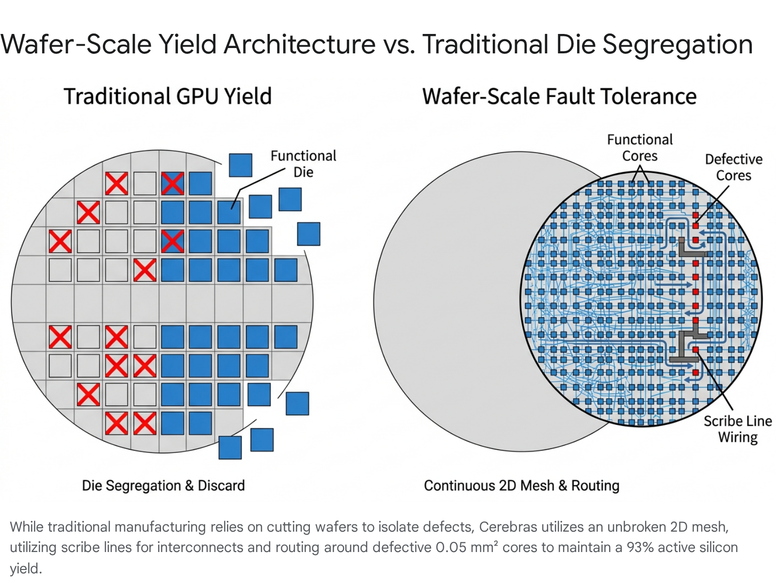
The primary historical barrier to wafer-scale computing has been defect density. In semiconductor fabrication, microscopic imperfections (such as dust particles or chemical irregularities) are inevitable. A traditional chipmaker mitigates this through dicing; if a 300mm wafer contains 50 defects, those defects might ruin 20 out of 70 diced chips, resulting in an acceptable yield for the remaining 50 functional chips 78. Because Cerebras requires the entire wafer to function as a single unit, traditional yield economics dictate that a single wafer-scale chip has a near 100% probability of containing fatal defects, ostensibly rendering every manufactured wafer defective 21.
Cerebras solves this problem through radical redundancy and a highly granular, fault-tolerant microarchitecture. The WSE-3 is manufactured with 970,000 physical cores, of which only 900,000 are required to function to meet commercial specifications 723. When a defect is identified during post-fabrication testing, the hardware's automated routing logic maps around the broken core, treats it as a non-functional entity, and dynamically routes data to a functional neighbor 211314.
The mathematics underpinning this strategy relies heavily on the physical size of the individual cores. Cerebras cores are extremely small, measuring approximately 0.05 mm2 each 7. According to industry data, TSMC's 5nm process yields an average of roughly 0.001 defects per mm2 7. If one compares the total silicon area lost to a defect, the difference between architectures is stark. In a monolithic GPU like the NVIDIA H100, which has roughly 144 Streaming Multiprocessors (SMs) within its 814 mm2 die, a single defect can disable an entire SM structure measuring roughly 6.2 mm2 7.
By contrast, a defect on the WSE-3 only disables a 0.05 mm2 core. When normalized across an equivalent total silicon area, the traditional GPU architecture sacrifices over 160 times more silicon to defects than the WSE-3 7. Across the 46,225 mm2 wafer, applying the 0.001 defect rate results in an expectation of approximately 46 scattered defects 7. Because each defect disables only 0.05 mm2, the total silicon lost across the entire wafer is roughly 2.2 mm2 7. Through this defect mapping, Cerebras achieves a 93% active silicon utilization rate across the wafer, an unprecedented metric for a chip of this magnitude 7.
Scribe Line Interconnects and Fabrication Economics
To achieve uniform connectivity across the entire wafer, Cerebras engineering implements a novel networking technique that repurposes the unused silicon "scribe lines" - the empty channels traditionally reserved for the mechanical saw blade during the dicing process. Working with TSMC, Cerebras deposits high-level metal layers over these scribe lines to create a continuous, ultra-low-latency 2D mesh data fabric spanning the entire 46,225 mm2 area 152326. This design effectively creates die-to-die connections without crossing package boundaries, avoiding the latency and power consumption associated with external network transceivers or optical interconnects 15.
The exact manufacturing cost per functional WSE-3 remains proprietary, but industry baseline estimates place raw TSMC 5nm/4nm 300mm wafer costs between $17,000 and $20,000 815. However, the true hardware cost of the Cerebras system is not strictly the raw silicon, but the heavy amortization of non-recurring engineering (NRE) costs, custom tooling, and the highly specialized packaging required to deploy a wafer-scale chip. By contrast, a single NVIDIA B200 logic die fabrication is estimated to cost between $720 and $1,200, supplemented by advanced CoWoS-L packaging ($1,000 to $1,200) and expensive HBM memory ($2,800 to $3,100), leading to a total module manufacturing cost of roughly $6,400 before retail markup 8.
| Manufacturing Metric | Cerebras WSE-3 | NVIDIA H100 GPU | NVIDIA B200 GPU |
|---|---|---|---|
| Silicon Area | 46,225 mm2 (Monolithic) | 814 mm2 | ~1,600 mm2 (Dual-Die) |
| Process Node | TSMC 5nm | TSMC 4N | TSMC 4NP |
| Transistor Count | 4 Trillion | 80 Billion | 208 Billion |
| Active Compute Cores | 900,000 | 16,896 | Not explicitly disclosed |
| Core Size | 0.05 mm2 | ~6.2 mm2 (SM) | Not explicitly disclosed |
| Inter-die Networking | Scribe line metal layers | NVLink 4 (External) | NVLink 5 (External) |
| Yield Management | Software routing around defects | Wafer dicing and binning | Wafer dicing and binning |
Data aggregated from manufacturing and architecture disclosures 71581022.
Data Center Infrastructure and Power Delivery
The extreme physical scale of the WSE-3 poses unprecedented mechanical, electrical, and thermal engineering challenges. While NVIDIA GPUs draw substantial power, their modular nature allows for distributed thermal management across standard server racks. Cerebras, conversely, concentrates an entire cluster's worth of processing power into a single physical unit. A single WSE-3 housed within the CS-3 system operates at roughly 23 to 25 kilowatts (kW) of power, requiring up to 30,000 amps of electrical current 14101316.
Three-Dimensional Power Distribution
Standard data center GPUs receive power laterally through the motherboard and peripheral component interconnect express (PCIe) slots, aided by bulk capacitors located adjacent to the chip on the printed circuit board. This lateral power delivery model is physically impossible for the WSE-3; power traveling sideways from the edges of a 46,225 mm2 silicon wafer would suffer from severe voltage drops, impedance, and catastrophic thermal issues before ever reaching the center cores 13.
To resolve this, the Cerebras CS-3 chassis mounts the power delivery network directly perpendicular to the wafer, utilizing the Z-axis. The architecture features front-side alternating current to direct current (AC/DC) modules, creating a dense 3D power distribution grid. An array of closely positioned voltage regulators sits directly above the silicon, delivering 30,000 amps of current vertically down into the wafer 13.
This massive concentration of current creates operational hazards during workload execution. When thousands of cores complete a highly intensive mathematical operation - such as a large matrix multiplication - and suddenly switch off, the instantaneous drop in power draw can cause destructive current spikes. To protect the circuitry, the CS-3 employs dynamic control logic that detects abrupt workload conclusions and rapidly injects "dummy operations" into the cores. These operations consist of multiplying random numbers to smooth out the power ramp-down, maintaining electrical stability across the wafer 13.
Thermal Management and Liquid Cooling
The thermal density of a 23 kW to 25 kW chip necessitates advanced, non-standard thermal management. While a standard 10U NVIDIA DGX B200 server features 8 GPUs drawing approximately 14.3 kW collectively and can be air-cooled in highly optimized facilities, a fully integrated NVIDIA GB200 NVL72 rack demands up to 120 kW, mandating liquid cooling infrastructure 162930. Industry guidelines standardly classify any rack exceeding 15 kW to 20 kW as high-density, triggering requirements for liquid cooling solutions 30.
The CS-3 engine block manages its thermal load using a closed-loop internal liquid cooling system equipped with redundant pumps 1017. Chilled liquid circulates directly over the silicon substrate through precision cold plates, removing the concentrated heat via conduction without relying on air as an intermediary 3032. The warmed liquid is then passed to an internal heat exchanger. From there, the heat can either be dissipated by high-velocity internal fans - allowing the CS-3 to integrate into air-cooled data centers utilizing rear-door heat exchangers - or tied directly into modern facility water systems 1017.
Datacenter infrastructure partners have begun designing specific environments for wafer-scale deployment. Nautilus Data Technologies, for instance, has deployed the CS-3 at its Stockton facility using a zero-water consumption ecological cooling loop. This system effectively manages the massive >20 kW per rack thermal load while adhering to stringent environmental sustainability targets and lowering the facility's Power Usage Effectiveness (PUE) 303218.
Network Scalability and Memory Architecture
While the WSE-3 relies entirely on its 44 GB of on-die SRAM to eliminate the memory bandwidth bottleneck during computation, 44 GB is fundamentally insufficient to hold the parameter weights of frontier large language models, which routinely exceed hundreds of billions of parameters 1021. NVIDIA addresses model size requirements by networking multiple GPUs, pooling their adjacent High Bandwidth Memory (HBM) via NVLink switches, and dividing the model using complex tensor and pipeline parallelism strategies 15922.
Cerebras solves the memory capacity constraint through a "decoupled memory" architecture. The CS-3 compute node is paired with external storage appliances known as MemoryX, which can be configured with 12 terabytes to 1.2 petabytes of memory 111617. A fully configured 1.2 PB MemoryX unit can store models with up to 24 trillion parameters without requiring the model to be partitioned or refactored 1216.
During execution, the model's layers are streamed sequentially from the MemoryX unit directly into the WSE-3 via a proprietary, high-bandwidth interconnect fabric called SwarmX 121719. Because an entire neural network layer fits comfortably within the 900,000 cores of the WSE-3, the operation is executed in pure data-parallel mode 1535. This architecture scales remarkably well; up to 2,048 CS-3 nodes can be clustered together using SwarmX, yielding near-linear performance scaling. This contrasts with traditional GPU clusters, where cross-node communication overhead over ethernet or Infiniband leads to diminishing returns as the cluster size grows 111617.
| Data Center Infrastructure Metric | Cerebras CS-3 System | NVIDIA DGX B200 (8-GPU Server) | NVIDIA GB200 NVL72 (Rack) |
|---|---|---|---|
| System Power Consumption | ~23 kW | 14.3 kW | ~120 kW |
| Peak AI Compute (FP16) | 125 PetaFLOPS | 36 PetaFLOPS | 360 PetaFLOPS |
| Memory Capacity | 1.2 TB to 1.2 PB (MemoryX) | 1.5 TB (HBM3e) | 13.5 TB (HBM3e) |
| Thermal Management | Closed-loop internal liquid | High-velocity air cooling | Direct-to-chip liquid cooling |
| Cluster Interconnect | SwarmX | NVLink / Infiniband | NVLink / Infiniband |
| Parallelism Model | Pure Data Parallelism | Data, Tensor, & Pipeline | Data, Tensor, & Pipeline |
Data compiled from technical whitepapers and deployment specifications 1016291920.
Artificial Intelligence Inference Economics
While Cerebras was initially engineered and positioned as an AI training accelerator for national laboratories and supercomputing centers, its fundamental economic proposition has pivoted sharply toward AI inference. Specifically, the architecture targets low-latency token generation for reasoning-intensive, long-context, and autonomous agent applications 33738.
Memory Bandwidth and Token Generation Speed
In large language model inference, generating a single new token (known as the "decode" stage) is fundamentally memory-bandwidth bound, rather than compute-bound 2121. Generating one token requires sweeping the entire set of model weights from memory through the compute cores 21. For a 70-billion parameter model utilizing 16-bit precision (FP16), the weights occupy approximately 140 GB 921. An NVIDIA H100 GPU, operating with 3.35 TB/s of memory bandwidth, is theoretically capped at generating roughly 24 tokens per second (at a batch size of 1) before accounting for interconnect overhead 9. The subsequent NVIDIA B200 improves upon this bottleneck with 8 TB/s of bandwidth and native FP4 precision, which effectively halves the memory footprint and doubles bandwidth utilization 922.
The Cerebras WSE-3 bypasses this limitation entirely. Because the model weights are streamed and resident immediately adjacent to the compute cores in SRAM, the system achieves 21 PB/s of on-chip memory bandwidth 1423. Independent benchmark tests conducted by Artificial Analysis demonstrate that on the Meta Llama 3.1-70B model, the CS-3 achieves inference output speeds of approximately 2,100 tokens per second per user, representing a 3x performance boost over previous software iterations and substantially outpacing generalized GPUs 2241.
On more complex architectures, such as the 400-billion parameter Llama 4 Maverick (a Mixture-of-Experts model), the CS-3 logged over 2,522 tokens per second per user 101421. By contrast, the flagship NVIDIA DGX B200 reaches roughly 1,000 tokens per second on the identical Llama 4 workload 31421. Similarly, on the OpenAI GPT-OSS 120B model, the CS-3 achieved 2,700 tokens per second compared to 900 tokens per second on the B200 1021.
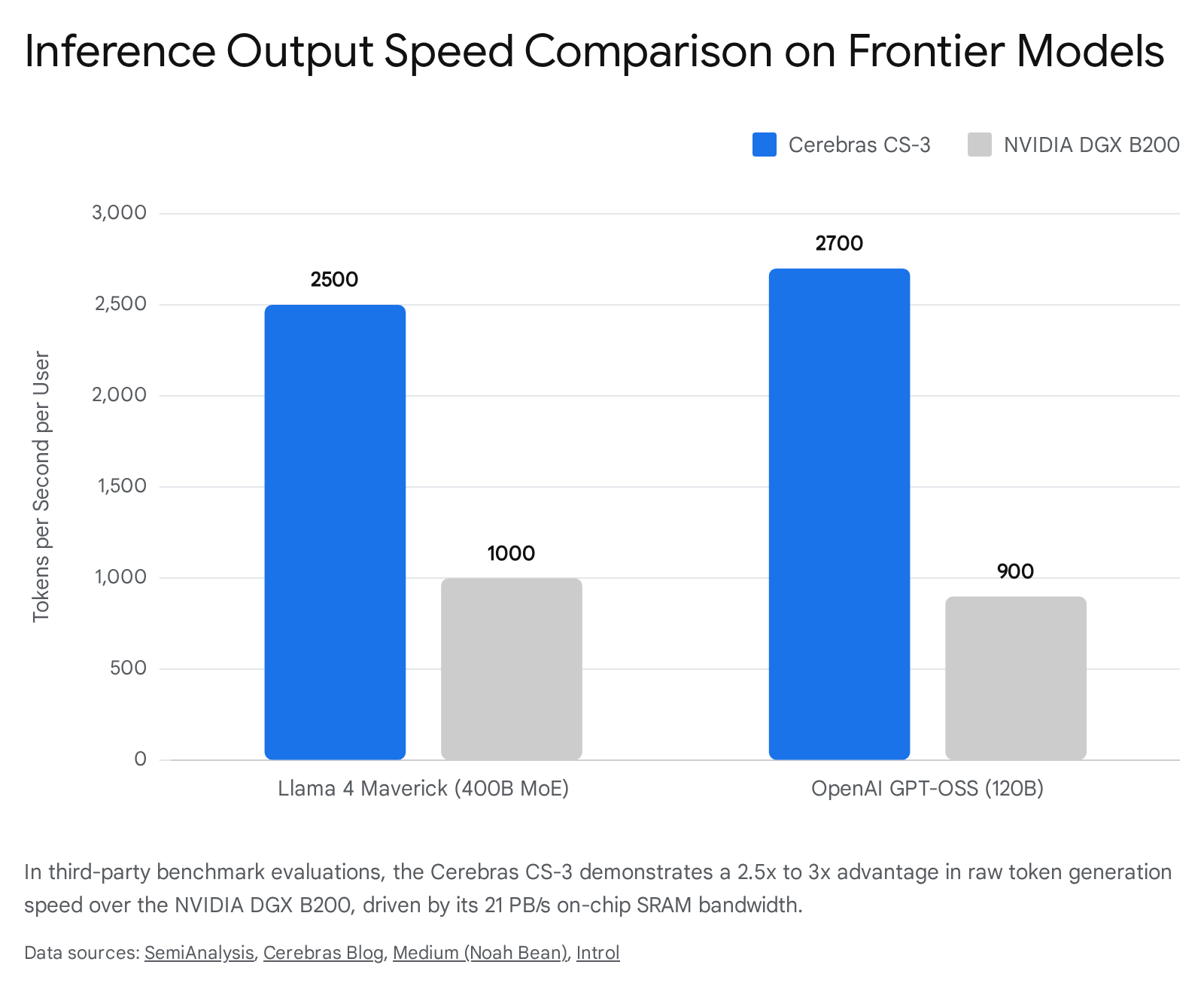
This immense speed advantage translates directly to reductions in Time-to-First-Token (TTFT) and total conversational response time. For agentic workflows or chain-of-thought models that execute dozens of internal reasoning steps before outputting a final answer, end-to-end latency dictates the viability of the software product 152122.
Hardware Cost and Throughput Efficiency
While the absolute speed advantage of the WSE-3 is clearly documented, the underlying unit economics of the hardware - specifically, the throughput generated per dollar of capital expenditure - remains an intensely debated topic within the engineering community.
Cerebras prices its API access aggressively to capture market share, charging $0.60 per million output tokens for Llama 3.1-70B and $0.10 per million for Llama 3.1-8B 42. However, translating this commercial API pricing to hardware Total Cost of Ownership (TCO) requires rigorous assumptions regarding hardware pricing, power costs, and utilization rates.
Estimates for the capital cost of a single CS-3 node range between $2.0 million and $3.0 million 151523. Some community analyses postulate that hosting a massive model like Qwen3-235B (with 131,000 context support) entirely within SRAM would require an array of 45 CS-3 chips, totaling upwards of $135 million, compared to an estimated $1 million for two DGX B200 systems capable of holding the same parameter weights in HBM 23. Cerebras officials have strongly disputed these figures, arguing that the MemoryX streaming architecture negates the need to hold the entire model simultaneously in SRAM, thus requiring far fewer CS-3 nodes to serve massive models efficiently 23.
The ultimate economic determinant is batch size. NVIDIA GPUs suffer from low throughput at batch size 1 (single-user queries), generating approximately 8 to 10 tokens per second on a single H100 for a 70B parameter model due to the memory wall 24. However, GPUs excel at high-batch processing. By batching 64 concurrent requests, an H100 cluster distributes the memory bandwidth penalty across multiple queries, achieving an aggregate system throughput of 120 to 150 tokens per second per card, or 800 to 1,000 tokens per second across an 8-GPU cluster 24.
Cerebras processes exceptionally fast at low batch sizes (hundreds of tokens per second at batch size 1), but the scaling curve for massive batching differs due to the monolithic nature of the data execution path 24. Consequently, the economic viability of Cerebras hinges on its utility for high-value, latency-sensitive tasks. For long-context workloads exceeding 100,000 tokens, or multi-step agentic workflows where response time dictates product viability, Cerebras asserts a 20% to 40% TCO advantage over GPU clusters due to energy savings and a reduced physical data center footprint 2124. For standard, high-batch asynchronous processing where latency is secondary, NVIDIA architectures generally maintain a cost-per-inference advantage 24.
| Inference Batch Size (70B Model) | Cerebras CS-3 (Tokens/sec) | NVIDIA H100 Single (Tokens/sec) | NVIDIA H100 8x Cluster (Tokens/sec) |
|---|---|---|---|
| Batch Size 1 | 25 - 35 (Est. scaling) | 8 - 10 | 15 - 20 (Limited by tensor parallel overhead) |
| Batch Size 8 | 180 - 250 | 40 - 50 | N/A |
| Batch Size 64 | 600 - 900 | 120 - 150 | 800 - 1,000 |
Data estimates derived from independent community benchmarks and hardware deployment analyses 24. Note: Raw token throughput varies significantly based on precision (FP16 vs FP8/FP4) and optimization frameworks.
Software Ecosystem and Competitive Moats
Hardware supremacy in the semiconductor industry is historically subservient to software entrenchment. Despite the physical advantages of wafer-scale integration, Cerebras faces significant adoption hurdles rooted in developer familiarity and existing codebases.
The CUDA Architecture Friction
NVIDIA's primary defensive moat is CUDA (Compute Unified Device Architecture) - a comprehensive, proprietary stack of compilers, runtime libraries, and mathematical optimization tools developed over more than 15 years 244546. For AI researchers training novel architectures, writing custom CUDA kernels ensures maximum hardware utilization on GPUs. Transitioning to a new accelerator requires abandoning this mature, battle-tested toolchain 244525.
Cerebras approaches this friction through abstraction. Its software stack, CSoft, acts as a custom compilation layer that directly ingests standard PyTorch and TensorFlow models 24. Because the WSE-3 operates as a single logical device, CSoft bypasses the need for the complex distributed systems code (e.g., NCCL, model parallelism scripts) required to partition workloads across NVIDIA GPU clusters 35214626. Training a massive model on Cerebras requires a fraction of the code overhead; for example, setting up a 175-billion-parameter model on a GPU cluster might require 20,000 lines of distributed computing code, whereas Cerebras can accomplish the identical setup with 565 lines 26.
PyTorch Integration and Migration Timelines
Despite this abstraction, adoption remains bifurcated based on the complexity of the user's software. For organizations deploying standard, well-documented transformer models (e.g., Llama, Mistral, GPT variants), CSoft compiles the PyTorch models natively and efficiently within a matter of days or a week 2445.
However, for research teams utilizing highly customized neural network architectures that rely on bespoke CUDA kernels, direct PyTorch inference on Cerebras is not automatically supported. Porting these complex models requires manual rewriting to adhere to the operations supported by the CSoft compiler. This process incurs a time-to-production delay estimated between 8 and 16 weeks, often necessitating extensive (and costly) vendor consulting engagements with Cerebras engineers to achieve optimal utilization 24.
In the inference market, the CUDA moat is arguably shallower 46. End-users of an inference API or a cloud endpoint prioritize token generation speed, accuracy, and cost, remaining largely agnostic to the underlying compiler operating in the data center. By wrapping its hardware in accessible, OpenAI-compatible inference services and partnering directly with hyperscalers like AWS to offer models via Amazon Bedrock, Cerebras is successfully circumventing the developer friction that previously hindered its adoption in the model training market 54546.
Comparative Financial Multiples and Market Positioning
Evaluating Cerebras's initial $39.8 billion baseline valuation and subsequent $48.8 billion IPO pricing necessitates a financial comparison against publicly traded peers NVIDIA and Advanced Micro Devices (AMD). The semiconductor market actively debates whether Cerebras's current valuation represents a justified "first-mover" premium for a revolutionary architecture or an over-extension driven by broader AI market exuberance 449.
Competitor Valuation Profiles
As of mid-2026, NVIDIA trades at a forward Price-to-Earnings (P/E) multiple of approximately 25x, supported by an annualized revenue run rate exceeding $215 billion and an 88% market share in data center accelerators 254927. This multiple reflects a market consensus that NVIDIA's earnings growth is sustainable, granting it a trailing Price-to-Sales (P/S) ratio fluctuating between 19x and 23x 2852. Furthermore, analyzing NVIDIA through the lens of the Price/Earnings-to-Growth (PEG) ratio yields an attractive 0.7 to 1.0, indicating that despite its massive $3.0 trillion-plus market capitalization, its valuation remains grounded relative to its 65% growth rate 2753.
AMD, fighting for the second-place position with its MI300 series accelerators, commands a significantly higher forward P/E multiple of approximately 84x and a trailing P/S ratio ranging from 18x to 22x 25295556. This elevated valuation reflects the market's expectation of rapid market share capture against NVIDIA, pricing in substantial future growth despite trailing revenues of roughly $22.8 billion 2556. AMD's PEG ratio sits higher, between 1.0 and 1.5, indicating a riskier, higher-reward profile 53.
Cerebras operates at a vastly different scale and trades at hyper-growth, speculative multiples. Assuming a $48.8 billion to $52.0 billion market capitalization and $510 million in trailing 2025 revenue, its P/S ratio hovers precipitously near 95x to 100x 330. Even when aggressively modeling forward revenue based on the rapid fulfillment of its $24.6 billion backlog - assuming straight-line revenue recognition of approximately $1.85 billion annually over the next two years - analyst estimates place its forward P/S between 17x and 36x 9. Using trailing net income, its P/E ratio is estimated at a staggering 222x 3.
Despite these stretched fundamental multiples, Wall Street brokerage firms initiated coverage of Cerebras with bullish outlooks following the expiration of the post-IPO quiet period. Morgan Stanley issued an "Overweight" rating with a $250 price target, citing the company's first-mover advantage in reasoning-intensive, low-latency inference 437. Citigroup was even more optimistic, assigning a 12-month price target of $340, which implies significant upside from initial trading levels and validates institutional confidence in the execution of the $20 billion OpenAI contract 43758.
| Financial Metric (Mid-2026) | Cerebras Systems (CBRS) | NVIDIA (NVDA) | AMD (AMD) |
|---|---|---|---|
| Market Capitalization | ~$40B to $52B 153 | ~$3.0T+ | ~$250B - $280B |
| Trailing Revenue (12m) | $510.0 Million (2025) 4 | ~$215.9 Billion 2527 | ~$22.8 Billion 56 |
| Trailing Price/Sales (P/S) | ~95x - 100x 330 | ~19x - 23x 2852 | ~18x - 22x 555659 |
| Forward P/E Ratio | ~222x (Trailing/Adjusted) 3 | ~25x 2560 | ~84x 25 |
| Strategic Target Market | Low-latency inference, sovereign AI | Broad hyperscaler infrastructure | Alternative GPU deployments |
Note: Multiples fluctuate based on daily market conditions; figures reflect aggregated analyst benchmarks post-IPO in mid-2026. Cerebras P/S reflects the high premium applied to early-stage, backlog-heavy revenue profiles.
At a valuation baseline approaching $39.8 billion to $50 billion, Cerebras Systems represents a high-conviction market bet that the architectural limitations of networked GPUs - specifically the memory bandwidth constraints restricting large language model decode speeds - cannot be solved incrementally. By keeping 44 GB of SRAM on a single 46,225 mm2 die and utilizing scribe line wiring, Cerebras delivers 21 PB/s of bandwidth, resulting in inference speeds up to 3x faster than NVIDIA's state-of-the-art DGX B200 on advanced reasoning models 141521. The financial viability of this premium valuation rests strictly on operational execution: Cerebras must successfully transition its staggering $24.6 billion backlog into realized revenue while scaling its highly specialized liquid-cooled data center infrastructure 341430. While NVIDIA remains the undisputed backbone of general AI computing, Cerebras has established wafer-scale integration as a premier physical architecture for the next generation of latency-bound, real-time artificial intelligence.