
How a Taiwan Crisis Could Affect Global Chip Supplies
A disruption in Taiwan would devastate the global technology supply chain, costing the world economy up to $10 trillion annually and grinding the production of everything from AI data centers to smartphones and vehicles to a halt. While the United States, Europe, and Japan are investing hundreds of billions to onshore chip production, the global economy will remain fundamentally dependent on Taiwanese advanced manufacturing and packaging through at least 2030. Rather than replacing Taiwan's dominance, current global investments are merely reshaping the island's "silicon shield" into a more distributed - but still highly vulnerable - network of geopolitical interdependence.
The Architecture of the Semiconductor Economy
To understand why the global economy is overwhelmingly dependent on a single island of 23 million people, one must first understand how the semiconductor industry fundamentally reorganized itself over the past three decades. The production of a single computer chip is arguably the most complex manufacturing process in human history. A modern semiconductor requires more than 1,000 distinct production steps, passing across international borders 70 or more times before ever reaching an end customer 1.
As the industry grew toward an estimated $1 trillion global valuation by 2030, this extreme complexity forced a fracturing of the semiconductor ecosystem into highly specialized business models 22.
The Fabless, Foundry, and IDM Divide
Historically, semiconductor companies designed, manufactured, and packaged their own chips. Today, the industry is broadly divided into distinct operational models. To use an industry analogy, if producing a chip is like baking a highly complex pastry, the "Fabless" company dreams up the recipe, while the "Foundry" acts as the massive, specialized bakery that actually cooks it 3.
| Business Model | Industry Role | Key Examples | Strategic Vulnerability |
|---|---|---|---|
| Fabless | Focuses exclusively on chip design and software architectures. Outsources all physical manufacturing to third parties. | Nvidia, Apple, AMD, Qualcomm | Entirely dependent on external foundries and packaging firms for physical product realization. |
| Foundry | Manufactures chips as a service for fabless clients. Does not design its own branded chips. | TSMC, GlobalFoundries | Requires massive capital expenditure ($20B+ per fab) and high utilization rates to survive market cycles. |
| IDM (Integrated Device Manufacturer) | Vertically integrated operations. Designs, manufactures, and packages its own chips in-house. | Intel, Samsung, Texas Instruments | Struggles to maintain simultaneous leadership in cutting-edge design, lithography, and manufacturing yields. |
| OSAT (Outsourced Semiconductor Assembly and Test) | Handles the back-end processes of packaging the silicon die and testing it for quality assurance before shipping. | ASE, Amkor, JCET | Vulnerable to supply chain disruptions and highly sensitive to material cost inflation. |
| Design House / IP Provider | Provides foundational intellectual property or "bridges" the gap by translating a fabless design into instructions the foundry can execute. | Arm, Synopsys, Cadence | Highly dependent on the continued growth of the fabless market and ecosystem standardization. |
The rise of the "fabless" model enabled explosive innovation in artificial intelligence and mobile computing. Companies like Nvidia and Apple save billions by avoiding the capital-intensive business of building fabrication plants (fabs) 46. However, this model resulted in a massive consolidation of manufacturing power. Taiwan Semiconductor Manufacturing Company (TSMC) pioneered the pure-play foundry model and today manufactures roughly 90% of the world's most advanced logic chips 5.
Beyond Moore's Law: The "Nanometer" Myth
When discussing advanced semiconductors, industry roadmaps frequently reference 5-nanometer (5nm), 3nm, or 2nm "nodes." For the general public, this implies a physical measurement of the transistor's gate length 6. In the early days of Moore's Law - the observation that transistor density doubles roughly every two years - this measurement was physically accurate. However, that reality jumped off the rails decades ago 7.
As the industry pushed into the deep ultraviolet (DUV) lithography era in the 1990s, the relationship between the node name and the physical gate length vanished 78. Today, process nodes are commercial marketing terms used to denote density, performance, and power efficiency equivalencies across different manufacturers 910. A transition from a 5nm to a 3nm process node essentially means the new chip architecture can perform more calculations while drawing less power and generating less heat - critical metrics for the hyperscale data centers driving the 2026 artificial intelligence boom 13.
Pushing the boundaries of these advanced nodes requires extreme ultraviolet (EUV) lithography systems - produced exclusively by ASML in the Netherlands - and incredibly precise manufacturing environments 911. This is a domain where Taiwan currently holds a near-insurmountable lead, commanding over 78% of the global foundry market 12.
The Hidden Chokepoints in Taiwan's Supply Chain
Taiwan's dominance is often framed as a triumph of engineering and clustered talent. However, running the world's most advanced fabs requires a massive, uninterrupted flow of physical resources. The island's vulnerability is not just military; it is deeply environmental and logistical.
The Thirst for Ultra-Pure Water and Energy
Advanced chip manufacturing requires ultra-pure water (UPW) to clean wafers between the hundreds of lithography, etching, and deposition steps. Contaminants measured in parts-per-billion can ruin entire batches of expensive silicon 13. As chips scale down to 3nm and 2nm, the number of necessary cleaning cycles increases dramatically; a single 3nm chip requires over 50 cleaning cycles during fabrication 13.
The scale of this consumption is staggering. TSMC's facilities at the Southern Taiwan Science Park alone consume roughly 99,000 tonnes of water daily - equivalent to the consumption of a city of 170,000 U.S. households 13. During the severe 2021 drought, Taiwan's fabs were forced to buy truckloads of water to maintain operations, a stark preview of chronic, climate-driven vulnerabilities 13.
Energy presents an even more immediate chokepoint. Taiwan is heavily dependent on imported energy, relying on foreign sources for 97% of its needs 5. Crucially, the island maintains a liquefied natural gas (LNG) reserve of only about 11 days 5. In comparison, South Korea holds 52 days of LNG storage, and Japan holds about three weeks' worth 5. Because TSMC's advanced EUV lithography machines require immense, uninterrupted power - projected to consume 12.5% of Taiwan's total electricity by 2025 - any disruption to maritime shipping routes would cripple chip production within weeks, entirely independent of a kinetic military strike 513.
Raw Material Dependencies
While Taiwan dominates manufacturing, it imports the vast majority of its critical semiconductor materials. High-performance photoresists, metal sputtering targets, and specialty reactive gases must be shipped in from abroad 14. Japan dominates the production of photoresists with a 90% market share 1.
Furthermore, ongoing geopolitical instability in the Middle East poses a constant threat to supply chains. A third of the global helium supply - critical for cooling and processing - is processed in Qatar, and sulfur is derived from oil and gas refining 5. A disruption in the Strait of Hormuz might not automatically halt chip production, but it would ripple immediately through Taiwan's power costs and materials supply, radically altering the economics of building AI infrastructure globally 5.
The AI Bottleneck: Advanced Packaging
For decades, the primary method of improving computer performance was simply shrinking transistors to pack more onto a single piece of silicon. As physics makes this monolithic scaling increasingly difficult and expensive, the industry has aggressively pivoted to "advanced packaging" 15. By 2026, this packaging layer has become the single largest bottleneck in the global AI supply chain 1920.
Heterogeneous Integration: The CoWoS Revolution
Instead of trying to print one massive, perfect chip, engineers now print smaller, specialized "chiplets" and stitch them together. In traditional packaging, a single chip sits on a basic substrate. Advanced 2.5D packaging, such as TSMC's industry-leading CoWoS (Chip-on-Wafer-on-Substrate), places multiple chips - like a central logic GPU and stacks of high-bandwidth memory (HBM) - side-by-side on a highly dense silicon interposer that acts as a super-highway for data, mounted on a larger organic substrate. This integration highlights how multiple smaller 'chiplets' are combined into a single high-performance system, bypassing the physical limitations of a single monolithic die 212216.
This heterogeneous integration is mandatory for modern AI accelerators like Nvidia's H100 and Blackwell architectures. Without CoWoS, the massive memory bandwidth required to train large language models is simply impossible 1921. The memory bandwidth that usually throttles AI performance increases dramatically when HBM stacks sit mere millimeters from compute dies on a silicon interposer, rather than across a traditional printed circuit board 19.
However, the CoWoS process is incredibly complex and capacity-constrained. The silicon interposer itself limits the maximum size of the package 17. As demand for AI data centers exploded through 2025 and 2026, TSMC's CoWoS capacity was rapidly overwhelmed 18. Nvidia alone reportedly secured over 70% of TSMC's CoWoS-L capacity for 2025, creating a hard ceiling on global AI development for competitors lacking similar purchasing power 1918.
Beyond Silicon: CoPoS and Future Packaging
To solve the physical size limitations and massive costs associated with silicon interposers, the industry is transitioning toward new architectures. CoPoS (Chip-on-Panel-on-Substrate) moves the process from round silicon wafers to square glass or organic panels 1719. By replacing traditional circular wafers with square panels (ranging up to 750 * 620mm), area utilization rates jump to over 95%, allowing for larger chip complexes and improved thermal stability 19. Another variant, CoWoP, leverages high-tech PCB motherboards to replace conventional IC substrates, filling the gap for mid-to-high-end applications requiring a balance of performance and cost 17.
The 2026 Squeeze: AI is Eating the Supply Chain
While geopolitics dominates the long-term outlook, the immediate reality in 2026 is driven by raw market economics. The explosive buildout of AI infrastructure - led by hyperscalers like Microsoft, Amazon, Google, and Meta, driving Project Stargate and similar initiatives - has profoundly distorted the semiconductor market 182021.
The Memory Market Cannibalization
These tech giants are investing hundreds of billions of dollars into data centers, creating an insatiable demand for advanced AI accelerators and High-Bandwidth Memory (HBM) 213022. Because global fab capacity is finite, memory manufacturers like Samsung, SK Hynix, and Micron have aggressively reallocated their production lines away from standard dynamic random-access memory (DRAM) and toward highly profitable HBM 2023.
HBM is resource-intensive to produce. The transition requires complex Through-Silicon Via (TSV) packaging and consumes roughly three times the wafer area to produce the same gigabyte capacity as standard DDR5 23. Consequently, standard DRAM production lines are being rapidly converted, restricting the legacy memory supply that powers the broader economy 23.
The Impact on Consumer Electronics and Automotive
The ripple effects of this AI prioritization have been severe for standard consumers and downstream industries. In the first quarter of 2026 alone, standard DRAM contract prices increased by up to 95%, marking the largest quarterly increase in the industry's history, while NAND flash contract prices jumped nearly 60% 3324.
Because memory components make up a significant portion of a device's total manufacturing cost - accounting for up to 35% of a laptop's cost in 2026, up from historical norms of 16% to 20% - this silicon inflation is being passed directly to retail buyers 24. Consequently, the consumer electronics market is bracing for broad price hikes. Laptops, smartphones, and household appliances are seeing retail prices rise by 15% to 30% 222425.
The automotive sector is also being explicitly deprioritized by suppliers who favor AI data center customers 18. Analysts warn that this creates a new "semiconductor scarcity" that will directly impact automotive OEMs by late 2026, threatening the production schedules of vehicles reliant on advanced driver-assistance systems 18. The dynamic is clear: the AI boom is effectively crowding out the rest of the technology supply chain 2226.
Visualizing Disruption: Blockade vs. Quarantine Scenarios
The intense concentration of these manufacturing and packaging capabilities in Taiwan has made the island the most critical single node in the global economy. Security analysts, military planners, and economists have modeled various contingencies regarding mainland China and Taiwan, separating them broadly into two tactical categories: Quarantines and Blockades.
Forecasters at the Swift Centre currently assign a roughly 9% probability to a Chinese blockade of Taiwan by mid-2027 27. While the likelihood is deemed relatively low - given the extreme risks of escalation and economic blowback - the impact would be historically catastrophic 27.
Quarantine: The Lawfare Strategy
A quarantine is distinct from a blockade. Under international law, a quarantine is generally treated as a law enforcement action rather than a formal act of war 2829. In this scenario, Beijing could utilize the China Coast Guard to encircle Taiwan, asserting administrative sovereignty and claiming a right to inspect all incoming and outbound vessels for "contraband," weapons, or biological threats 29.
This operates as a grey-zone tactic, heavily reliant on lawfare. By controlling the customs process without necessarily firing a shot, China could drastically slow down maritime traffic 29. For the semiconductor industry, a quarantine introduces severe delays, spikes maritime insurance premiums, and disrupts the "just-in-time" delivery of critical precursor chemicals and gases 2940. However, because it is not an absolute siege, some trade may still flow, keeping fabs operating at diminished, heavily rationed capacities.
Blockade: The $10 Trillion Shock
A blockade is an absolute military siege, forbidding the movement of all air and maritime traffic, and constitutes a formal act of war 2829. If a blockade is sustained, the economic impact is near-instantaneous.
Because Taiwan relies on an 11-day LNG reserve, energy rationing would begin almost immediately 5. Advanced fabs cannot operate on intermittent power; temperature, vibration, and environmental controls must remain absolute 527. Production at TSMC would cease entirely 2740.
| Scenario Parameter | Estimated Impact | Core Economic Drivers |
|---|---|---|
| Direct Global GDP Loss | $5 Trillion to $10 Trillion annually (approx. 5% to 10% of global GDP) 3042 | Paralysis of the $1T semiconductor market; cascading shutdowns in global automotive, consumer electronics, and defense manufacturing. |
| Impact on Mainland China | Severe. $1.4 Trillion in Chinese trade passes through the Strait annually 31. | Over half of voyages through the strait are intra-China shipping. A blockade disrupts domestic Chinese supply chains and severs access to advanced chips 31. |
| TSMC Operational Status | Offline within 30 to 90 days 2740. | Rapid exhaustion of ultra-pure water feedstocks, specialty gases, and stable baseload power 527. |
Global economic losses in a full blockade scenario are estimated by Bloomberg Economics to reach $10 trillion in the first year alone 3042. A RAND Corporation study of a severe, prolonged conflict estimates global losses could climb as high as 15% of world GDP annually 30. The impact would be highly uneven, heavily punishing economies reliant on manufactured goods, but because semiconductors are the foundational hardware of the modern digital economy, no sector would be entirely insulated 30.
Crucially, China's own economy would suffer deeply. The Taiwan Strait is one of the world's busiest waterways, and an estimated $2.45 trillion worth of goods transited it in 2022 31. Of that, a staggering $1.4 trillion represented Chinese imports and exports 31. Furthermore, over half of all voyages through the strait are bound from one Chinese port to another, meaning a conflict would severely hamper domestic supply chains within mainland China 31.
The Erosion of the "Silicon Shield"
For years, Taiwan's geopolitical security strategy has been informally tied to the concept of the "silicon shield" - the idea that the island's absolute dominance in advanced chip manufacturing makes it so vital to the global economy that the United States and its allies would be forced to intervene militarily to protect it, while simultaneously deterring China from risking the destruction of the very supply chains it relies upon 3233.
However, as TSMC expands globally - building fabs in Arizona, Kumamoto, and Dresden - a vigorous debate has emerged within Taiwan. Does moving advanced manufacturing abroad erode the silicon shield? If the U.S. and its allies can source advanced chips domestically, will their willingness to incur military costs for Taiwan's defense diminish? 3435.
"Managed Diffusion" vs. Dilution
Taiwanese strategists increasingly view this international expansion not as a hollowing out, but as "managed diffusion" 35. Taiwan's strategic leverage does not rely purely on the geographic location of its factories, but on its absolute control over the cutting-edge technological frontier 35.
While TSMC builds 4nm and 3nm fabs abroad, it tightly retains its most advanced 2nm and future 1.4nm research, development, and high-volume manufacturing within Taiwan's borders 323637. Advanced manufacturing remains inseparable from continued access to Taiwan-based innovation, engineering talent, and process leadership 35.
By integrating Taiwanese operations into the domestic economies of the U.S., Japan, and Europe, Taipei hopes to institutionalize its alliances. The evolving silicon shield is designed so that a disruption in the Taiwan Strait would not just cut off an external supplier, but would directly paralyze the internal industrial policies and economic security of the world's most powerful democracies 3538.
The Danger of Overdependence
Domestically, however, Taiwan faces economic risks stemming from this very success. Recent tabletop exercises run by Taiwanese experts highlighted severe structural vulnerabilities 39. Information and communications technology (ICT) exports account for nearly 80% of Taiwan's total exports 39. This overwhelming reliance on the integrated circuit (IC) industry leaves the broader economy dangerously exposed to shifts in global semiconductor demand 39. Resources have become so heavily concentrated in the IC sector that it is crowding out traditional industries, contributing to uneven wage growth and leaving sectors like agriculture highly vulnerable to targeted economic coercion 3940.
The Great Onshoring: Reality vs. Ambition in 2026
Recognizing the existential risk of relying entirely on Taiwan, governments worldwide launched historic industrial policies to subsidize domestic manufacturing. However, as these policies hit the ground in 2025 and 2026, the reality of building advanced semiconductor ecosystems from scratch has proven far more difficult than passing legislation.
United States: Construction Delays and Yield Successes
The $52 billion U.S. CHIPS and Science Act aimed to revive domestic manufacturing, but the effort has been plagued by regulatory and market delays 4154. Building a fab in the U.S. is uniquely slow; a study of construction between 1990 and 2020 found that the average U.S. fab takes 736 days to build, significantly lagging behind Asian competitors 42.
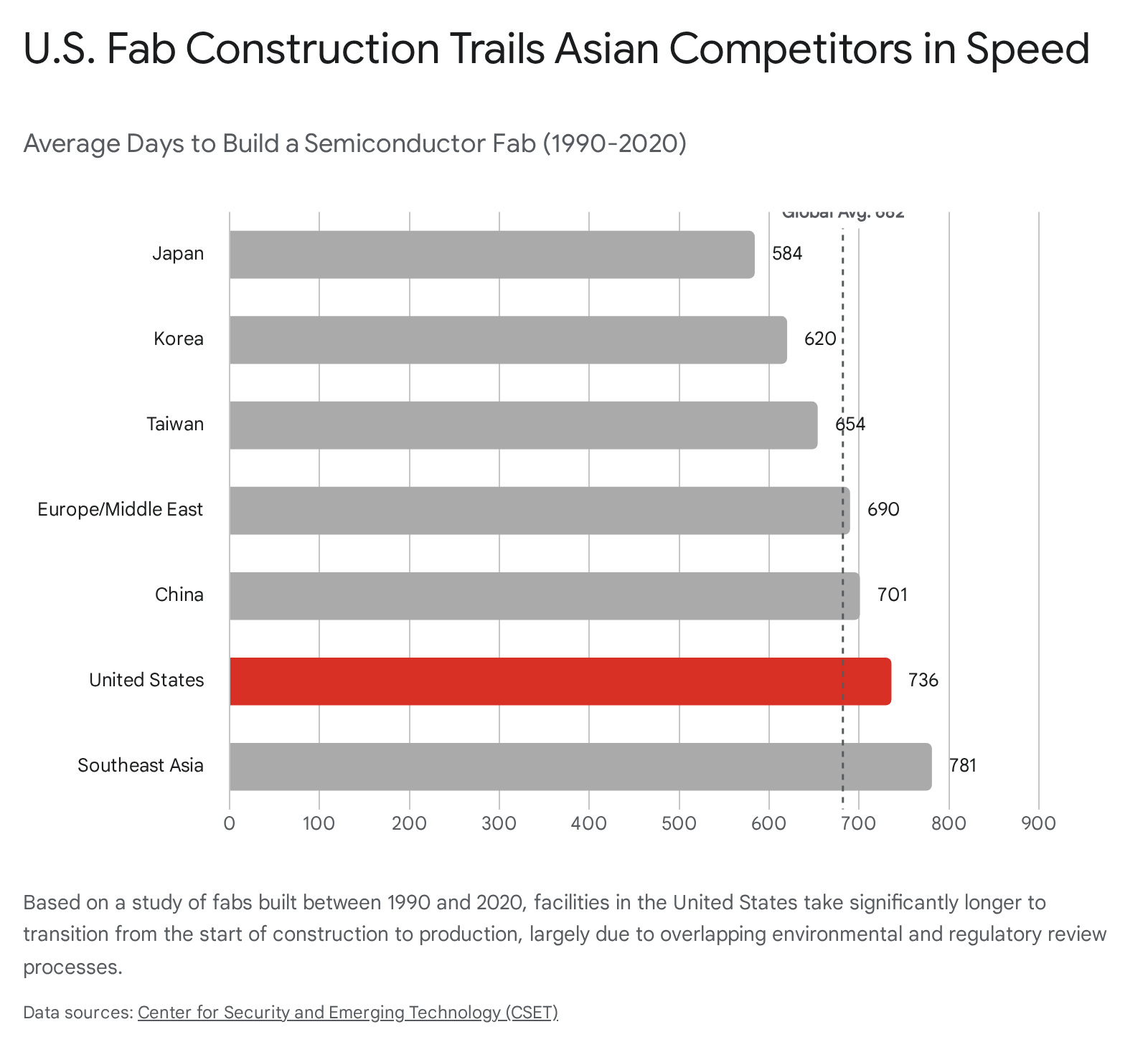
This delay is largely attributed to overlapping federal, state, and local environmental reviews (such as NEPA) and complex zoning regulations 4243.
Consequently, major U.S. projects faced timeline revisions. TSMC's second Arizona fab was pushed to 2028, and Intel's massive $20 billion "Silicon Heartland" mega-site in Ohio delayed production targets to the 2027 - 2030 window, citing changing market dynamics and labor constraints 5457. Samsung's Texas fab was similarly pushed from 2024 to 2026 54.
Despite these structural hurdles, by early 2026, the U.S. achieved significant operational milestones. TSMC's first Arizona facility (Fab 21) officially began producing 4nm and 5nm chips with yield rates exceeding 92% - matching its top-tier facilities in Taiwan 3457. This effectively disproved skeptics who believed American labor and engineering ecosystems could not match Asian efficiency for advanced logic 3457. Simultaneously, Intel successfully brought its 18A (1.8nm-class) process into high-volume manufacturing at its Ocotillo campus in Arizona, marking the historic return of leading-edge lithography to American soil and establishing a domestic "silicon shield" for advanced computing 57.
Japan's Twin Strategy: Mature Resilience and Advanced Ambition
Japan, once the dominant global semiconductor force in the 1980s, has pursued a highly subsidized, two-pronged strategy to regain its edge 1144. The government has deployed roughly 0.7% of its GDP toward semiconductor and AI support - a rate significantly higher than the U.S. CHIPS Act proportional to the economy 45.
First, the government heavily subsidized TSMC to build a joint venture fab in Kumamoto (JASM) in partnership with Sony, Denso, and Toyota 134647. This facility focuses on mature and mid-advanced nodes (ranging from 40nm down to 6nm) to securely supply Japan's robust automotive, robotics, and industrial electronics sectors 1348. This domestic collaboration is widely considered a massive success, progressing far faster than American or European counterparts 4446.
Second, Japan launched Rapidus, a government-backed consortium aiming to leapfrog directly from 40nm capabilities to 2nm mass production by 2027, in partnership with IBM and imec 1136. This approach relies heavily on global integration rather than domestic evolution 44. Rapidus is viewed as a high-risk system shock; Japan lacks a recent history in advanced logic manufacturing and faces a critical shortage of an estimated 40,000 semiconductor engineers 1346. Nevertheless, it represents one of the few credible attempts outside of the U.S., Taiwan, and South Korea to build a state-of-the-art logic foundry capable of competing with TSMC and Samsung 36.
Europe's Pivot to "Indispensability"
The European Union initially launched its €43 billion Chips Act with a highly ambitious, politically driven goal: to double its share of the global semiconductor market to 20% by 2030 4950.
By 2025 and 2026, European policymakers and auditors faced a harsh reality check. A report by the European Court of Auditors found the bloc "far off the pace" required to meet its ambitions 5051. Not only was the committed funding vastly insufficient compared to the estimated €120 billion required to restart competitive local production, but the global market was growing so fast that the EU's overall share of global value was projected to rise only slightly, from 9.8% in 2022 to just 11.7% by 2030 515267.
In response, the EU began pivoting toward a "Chips Act 2.0" strategy. Rather than striving for impossible self-sufficiency across all nodes, or attempting to blindly copy Taiwan in advanced sub-3nm logic, Europe's new strategy focuses on technological indispensability 4952. The core argument is straightforward: sovereignty means securing access by strengthening the specific parts of the value chain where Europe already matters 52. This means doubling down on industrial powerhouses like Bosch, Infineon, and NXP, which dominate the mature-node automotive and industrial chip sectors, and leveraging ASML's absolute monopoly on EUV lithography equipment to ensure global partners cannot afford to cut Europe out of the market 1167.
In late 2025, the European Commission formally granted "Integrated Production Facility" (IPF) and "Open EU Foundry" (OEF) status to several major projects, including a massive TSMC joint venture in Dresden (ESMC) and Infineon facilities, streamlining permitting processes and prioritizing administrative support to accelerate this localized strategy 5354.
Bottom line
The global semiconductor supply chain is currently defined by a severe tension between explosive AI-driven demand and extreme geographic vulnerability. While historic, multi-billion-dollar industrial policies in the U.S., Japan, and Europe are successfully establishing regional manufacturing footholds and proving that onshoring is technically possible, the staggering complexity of advanced packaging and resource-intensive fabrication ensures Taiwan will remain the indispensable core of the industry through at least 2030. Should a blockade or quarantine materialize before these global ecosystems fully mature, the economic devastation will be measured in trillions, stalling both consumer technology markets and the artificial intelligence revolution indefinitely.